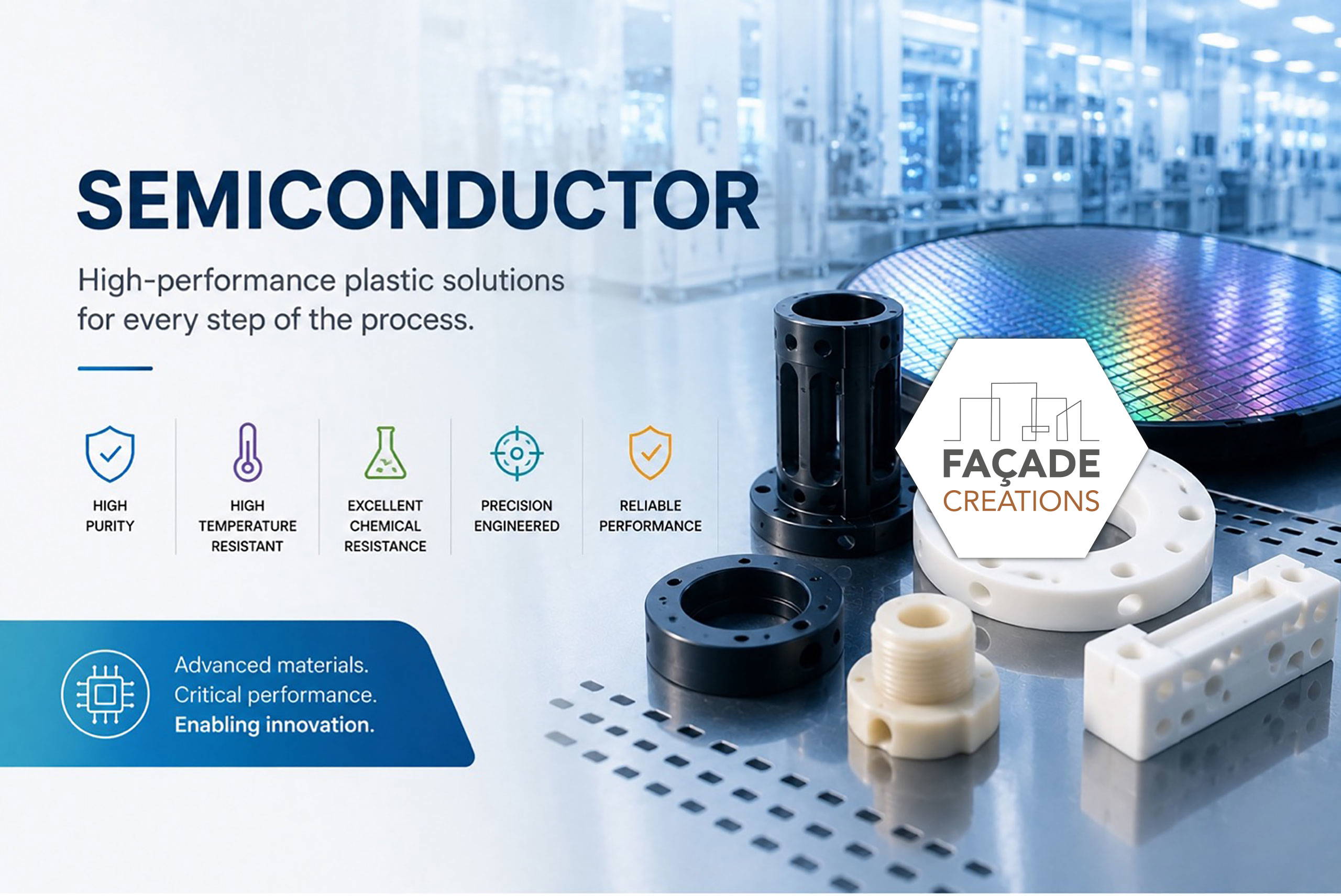
High-performance plastic solutions for semiconductor and electronics manufacturing
Façade Creations is a global manufacturer of engineering and high-performance plastic solutions for semiconductor and electronics manufacturing equipment and components. Our compounds, machinable shapes, and finished components made of advanced thermoplastics have a proven track record in almost all major semiconductor tools throughout the entire fabrication process, ranging from wet processes, chemical mechanical planarization, plasma etching, deposition, lithography, testing, assembly, packaging, and more.
Each stage of the fabrication process offers its own set of challenges: from extremely high temperatures, to exposure to highly aggressive chemicals, strictest purity requirements, tightest design and machining tolerances, or contact with plasma under vacuum. Working closely with many of the leading equipment and system manufacturers, Façade Creations has established a dedicated portfolio of specialised semiconductor plastics that withstand these harsh processing conditions while enhancing part performance, minimising contamination and defects, and lowering overall cost of ownership.
Get in touch with our team
(However, if you prefer to speak to someone directly? Call our aerospace team or email us and we’ll respond promptly.)
Team Contact Form
Benefits of Façade Creations Semiconductor Plastics
- Operation reliability
- Dimensional stability
- Production yield
- Supply reliability
Enhancing operation reliability with copy-exact materials and components
Façade Creations’ semiconductor materials and parts are processed in compliance with semiconductor “copy exact” requirements (also known as CE) and with the most stringent contamination and quality controls. Having the full value chain in-house – from raw material inspection, compounding, extrusion and compression moulding, machining and further processing – enables consistent traceability and semiconductor-specific quality inspections at every process step. Moreover, integrating the whole value chain allows for consistent copy-exact management, covering lockdowns and change notifications at all major internal process steps. In this way, Façade Creations ensures a level of cleanliness and quality performance consistency significantly above industry-standard materials, helping to secure reliable operation of semiconductor manufacturing equipment components.
Faster machining cycles and yield improvements through enhanced dimensional stability
High-performance plastics are often used for semiconductor manufacturing equipment parts that must maintain tight tolerances during fabrication and after prolonged use. Extruded plates in particular pose a great challenge in terms of the dimensional stability necessary to achieve such tight tolerances. Through optimisation of our manufacturing process, Façade Creations has succeeded in reducing internal stresses to levels not previously achieved. The result is a new generation of high-performance plastics capable of meeting the market’s highest application demands. Low internal stress leads to less bending and warpage during machining and in operation – particularly important for parts machined from plastic sheets that require high levels of flatness. This lower internal stress also enables faster speeds and feeds during machining, and can significantly reduce the need for intermittent post-annealing steps between operations. The result is faster part production and better yield, considerably reducing costs.
Improving production yield with thoroughly filtered and refined materials and components
Manufacturing high-performance plastics – PPS in particular – poses a great challenge in reducing visual defects such as black specks, streaks, flow marks and other impurities. Some demanding applications require high optical cleanliness of the part surface, and in certain semiconductor applications, impurities in the material can even have damaging effects on process yield. Façade Creations’ product lines for semiconductor manufacturing are produced under special conditions and specifications designed to minimise the risk of impurities or visual defects.
Securing reliable supply with global production and delivery capabilities
With production capabilities, warehouses and customer support centres across multiple locations in Europe, Asia and the Americas, Façade Creations has a strong track record of securing reliable supply for customers worldwide. Integrating the entire fabrication process under one roof – from compounding, moulding and further processing – helps minimise the risk of supply bottlenecks and manage supply performance more effectively. Close partnership and supply assurances with premier raw material suppliers also help us avoid delivery bottlenecks. Façade Creations runs efficient stock management and global demand planning systems to ensure a high level of availability and delivery performance for semiconductor materials.
Semi-Finished and Finished Parts for Semiconductor and Electronics Manufacturing
Products from Façade Creations for the semiconductor industry
- Shapes
- Compounds
- Filaments
Façade Creations offers a wide spectrum of engineering and high-performance plastic stock shapes for semiconductor and electronics manufacturing equipment parts. All our semiconductor-grade plastics are processed in compliance with copy-exact requirements and stringent contamination and quality controls, ensuring the highest level of cleanliness and quality performance consistency. Special measures during production also ensure low internal stress and enhanced dimensional stability during machining.
With hundreds of different dimensions available in stock, Façade Creations offers strong diversity to meet the semiconductor industry’s demands. This allows machine shops to choose the closest size, saving material waste and cost, and enabling overall component cost reductions. Lot sizes range from a single piece for prototyping projects to large industrial-size lots. Warehouses around the world extensively stock our semiconductor-grade materials, ensuring that even large quantities are delivered in the shortest possible time, or “just-in-time”.
Façade Creations develops and produces specialised compounds with a focus on high-performance and engineering thermoplastics. Our solutions for semiconductor and electronics manufacturing equipment include tribologically optimised materials (less wear, lower friction) and materials with defined electrical characteristics.
Façade Creations also produces filaments made from high-performance plastics for 3D printing. Stock materials are available, along with the option to develop customised filaments for prototyping or complex parts used in semiconductor and electronics manufacturing.
Finished parts from Façade Creations for the semiconductor industry
- Machined parts
- Injection-moulded parts
- Profiles
- Customised tubes
Façade Creations manufactures complex parts and assemblies for semiconductor and electronics manufacturing equipment across our global network of machine shops in Europe, Asia and the Americas. Our capabilities include machining, milling, micro-drilling, bonding, finishing, annealing for low-tension machining, engraving, assembly and further processing. Stringent copy-exact management and traceability enable the highest level of quality and performance consistency.
Façade Creations also manufactures precision parts and complete assemblies for semiconductor and electronics manufacturing equipment at our injection-moulding facilities. Our capabilities include multi-component injection moulding, insert/overmoulding, assembly, tool making, automation and further processing.
Plastic profiles are already used in many applications in the semiconductor industry, and the market is growing: profiles made of plastic offer advantageous mechanical, thermal and electrically insulating properties combined with low weight. We manufacture high-precision plastic profiles to customer specifications and can take your requirements for geometry, dimensions and material into account individually. In addition to custom-fit extruded profiles, we also offer high-strength continuous fibre-reinforced profiles, manufactured in-house using thermoplastic pultrusion.
In addition to our comprehensive stock programme, we also offer customised tubes, rods and hoses for semiconductor industry solutions, tailored specifically to your application.
Property Solutions for Semiconductor and Electronics Manufacturing Equipment Parts
Façade Creations’ semiconductor material solutions offer improvements in the following areas:
Strength and rigidity at high temperatures
Many components in semiconductor and electronics manufacturing and testing equipment require thermally resistant materials. Components in elevated-temperature environments must maintain high mechanical properties and dimensional stability, while keeping outgassing, leaching and particle generation to a minimum. Façade Creations’ high-temperature-resistant plastics can be used at service temperatures of up to 400°C depending on operating conditions. High-performance plastics are increasingly replacing ceramics and quartz in high-temperature applications due to lower risk of breakage, easier machinability and better cost performance.
Indicative long-term/short-term heat resistance by material family:
Ionic purity and low outgassing
Even the smallest trace amounts of foreign molecules, particularly metals, can cause severe process degradation and compromise yield. Especially in advanced processes with reduced nodes, using ultraclean materials for equipment components is key to minimising airborne molecular contamination (AMC) and particle contamination from material outgassing, leaching and particle shedding.
Façade Creations’ semiconductor material solutions are based on selected high-purity polymers with a proven track record in critical semiconductor manufacturing equipment components with wafer contact. The entire value chain – from raw material inspection, compounding and moulding through to further processing – takes place under special conditions and specifications designed to minimise the risk of impurities. Trace metal content across our polyimide, PEEK, PPS and PET-based grades is consistently held to very low parts-per-million levels, verified through ICP-MS testing.
Long-term performance in aggressive chemicals
Various harsh chemicals are used to process and clean wafers. Consequently, wet-process tool components need to provide adequate chemical resistance to ensure part performance, maximise component life and minimise contamination risk. Erosion of the part surface can destroy its net shape and contaminate the substrate with particles; chemical degradation also compromises mechanical properties and can result in critical part failures.
Façade Creations offers a wide range of plastics with high chemical resistance, suitable for almost all wafer processing environments. As a general guide, materials such as PPS and PTFE offer very strong resistance across most common wet-bench chemicals – including hydrofluoric acid, sulfuric acid and hydrogen peroxide – while PEEK and PEI offer good resistance to a broad range of solvents and acids, and PVDF performs particularly well against strong acids but less well against solvents such as acetone. Chemical resistance of plastic is highly dependent on temperature and operating conditions, so we’re happy to advise on the best material for your specific process chemistry.
Electrical static discharge (ESD) prevention
Electrostatic discharge (ESD) management is key for semiconductor and electronics manufacturing equipment, as particle attraction from electric charges or integrated circuit destruction from discharges can critically affect yield. Façade Creations’ extensive portfolio of electrically modified plastics has a proven track record in highly ESD-sensitive semiconductor and electronics manufacturing processes, such as wafer mobility components, chip transportation trays, IC test sockets and electronics fixtures.
- Conductive plastics – surface resistivity of 10² – 10⁴ Ω/sq, enabling materials to quickly bleed away electric charge
- Dissipative plastics – surface resistivity of 10⁶ – 10⁹ Ω/sq, enabling a slower, controlled rate of static charge decay
- Anti-static plastics – surface resistivity of 10⁹ – 10¹² Ω/sq, providing the minimum current decay rate among our electrically modified plastics
In addition to different conductivity levels, our broad range of polymers with different physical and thermal properties allows customers to find the best-matching material for their application’s needs.
Resistance to energetic plasma
In semiconductor manufacturing processes such as vapour deposition, dry etching or ion implantation, equipment components are exposed to highly aggressive and corrosive plasma under vacuum conditions. Some plasma processes operate at temperatures above 250°C, requiring equipment components to provide high thermal stability. Façade Creations’ semiconductor-grade polyimide materials are developed to offer superior plasma and temperature resistance compared to industry-standard polyimide and other high-performance plastics. Lower weight loss and etching speed at elevated temperatures enable longer part service life, reducing replacement shutdowns, while reduced material contamination enables significantly improved process yield.
Dimensional stability and micro-machinability
Many components in semiconductor and electronics manufacturing equipment require fine features with tight design and machining tolerances. Through optimisation of our manufacturing process, Façade Creations’ semiconductor-grade materials provide low internal stress levels, enabling superior dimensional stability during machining and in operation. Our semiconductor-grade materials are also based on selected polymers that provide high levels of dimensional stability in terms of thermal expansion, water absorption and mechanical stability.
Some high-end applications, such as IC test sockets and electronic inspection fixtures, require machined parts with micro holes, in some cases smaller than 0.1mm. As such applications require special material property profiles, Façade Creations has developed a dedicated portfolio with enhanced micro-machinability and dimensional stability.
Tribological and wear performance
Many components in semiconductor and electronics manufacturing and testing equipment are exposed to high sliding speeds and pressing forces. Choosing the right material is key, as a material’s wear performance directly impacts part lifetime, replacement cycles and maintenance costs. High abrasion and particle shedding can also cause excessive wafer contamination and significantly decrease process yield. Façade Creations’ plastic solutions have a proven track record in components requiring high resistance to wear and tear while providing high levels of cleanliness.
Latest regulatory requirements
For a company supplying globally to high-tech applications, only the highest level of product compliance is good enough. We continually invest in research and close cooperation with raw material suppliers and test institutes to stay ahead of today’s latest demands. Upon request, we can issue conformance declarations for a broad range of environmental standards, such as REACH and RoHS.
Application Examples
Wafer carrier
Injection-moulded from a natural PEEK material.
- Narrow tolerances
- High ionic purity and low outgassing
- High dimensional stability
- High strength and stiffness
- Good abrasion resistance
CMP stop edge ring
Machined from a natural PEEK tube.
- High ionic purity
- Copy-exact compliant
- High strength and stiffness
- Good abrasion resistance
- High dimensional stability
Wafer handling vacuum wand
Machined from an electrically conductive PEEK nano-grade material.
- Consistent electrical conductivity, ESD protection
- Good ionic purity
- Copy-exact compliant
- Good impact resistance
- Good abrasion resistance
Gas feed flange
Machined from a black, carbon-fibre-reinforced conductive PEEK material.
- Consistent electrical conductivity, ESD protection
- High strength and stiffness
- High creep resistance
- Good abrasion resistance
- Copy-exact compliant
Batch spray chamber
Machined from a natural PVDF material.
- Excellent chemical resistance
- Reduced material waste by machining from tube
- Good ionic purity
- Good dimensional stability, low water absorption
- Good mechanical strength compared with other fluoropolymers
Single wafer cleaner holding part
Machined from a black, electrically conductive PEEK nano-grade material.
- Consistent electrical conductivity, ESD protection
- High strength and ductility
- Good abrasion resistance
- Dimensional stability during machining
- Copy-exact compliant
Contact
We are happy to advise you individually on material selection and semiconductor solutions for your project.
Team Contact Form